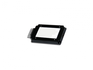
1X4 MEMS OSW Module Device


Request a Quote
Description
Product FunctionMEMS OSW is based on micro-electro-mechanical system (MEMS) technology, which achieved low insertion loss and highly repeatability by rotating the mirror of MEMS chip.
MEMS OSW is mainly used in optical cross and connection (OXC) system, optical add/drop system, measure instrument system and optical signal monitoring system.
The products are Telcordia GR-1073-CORE qualified, and RoHS compliant.
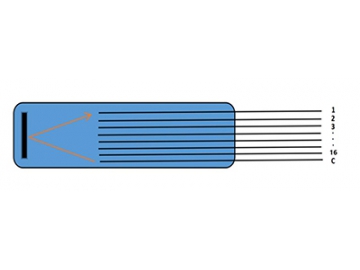
Product ConfigurationsNote: “C”: common port
“1、2、3...16”:possible selected output ports=1~16
Optic Specification
| No. | Parameters | Unit | Value | Notes |
| 2.1 | Wavelength | nm | 1528~1565 | or customer specify |
| 2.2 | Test Wavelength | nm | 1550 | - |
| 2.3 | OSW Channels | - | 4 | - |
| 2.4 | Insertion Loss | dB | ≤0.8 | @CWL,23°C, Without Connectors |
| 2.5 | Return Loss | dB | ≥40 | - |
| 2.6 | Repeatability | dB | ≤0.1 | - |
| 2.7 | Crosstalk | dB | ≥40 | - |
| 2.8 | Polarization Dependence Loss | dB | ≤0.2 | - |
| 2.9 | Wavelength Dependence Loss | dB | ≤0.3 | @CWL±20nm, 23°C |
| 2.10 | Temperature Dependence Loss | dB | ≤0.4 | - |
| 2.11 | Operation Temperature | °C | -5~70 | - |
| 2.12 | Storage Temperature | °C | -40~85 | - |
| 2.13 | Switch Time | ms | ≤30 | - |
| 2.14 | Durability | cycle | ≥1x10⁹ | - |
| 2.15 | Maximum optical Power | mW | ≤500 | - |
| 2.16 | Switch Mode | - | Non-latching | - |
| 2.17 | Control Voltage | V | 5±0.25v | - |
Operation/storage Temperature/humidity
| NO | PARAMETER | SPECIFICATION | UNITS | NOTE |
| 3.1 | Operation Temperature | -5~65 | °C | - |
| 3.2 | Storage Temperature | -40~85 | °C | - |
| 3.3 | Operation Humidity | 5~95 | %RH | - |
| 3.4 | Storage Humidity | 5~95 | %RH | - |
Pigtail and Connector
| NO | PARAMETER | SPECIFICATION | UNITS | NOTE |
| 4.1 | Fiber Type | G657A2 or G657B3 250um bare fiber | - | - |
| 4.2 | Fiber Pigtail(All Ports) | 900um loose tube | - | - |
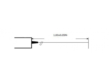
| 4.3 | Fiber Length(All Ports) (customer specify) | 1.00±0.05(customer specify) | m | with connector length |
| 4.4 | Optical Connector (All port) | None (customer specify) | - | - |
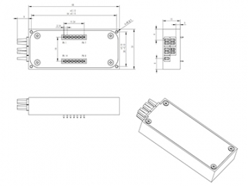
Mechanical Drawings
Optic Ports and Electronic Pins Definition
Electronic Pins Definition| Pin Number | Name | Input/Output | Level | Function |
| 1 | NC | No connect | - | - |
| 2 | VCC | Power supply | - | +(5.0±5%) V Power Supply Max 100mA |
| 3 | Strobe | Input | LVTTL | Reserved |
| 4 | GND | Power supply ground | - | Power supply ground |
| 5 | D0/A0 | Input | LVTTL | Reserved |
| 6 | TXD | Input/Output | LVTTL | For TTL Mode: Not used |
| For UART Mode: DATA output | ||||
| 7 | RXD | Input | LVTTL | For TTL Mode: Not used |
| For UART Mode: DATA input | ||||
| 8 | I/F Mode | Input | LVTTL | Reserved |
| 9 | D2/A2 | Input | LVTTL | Reserved |
| 10 | /Done | Output | LVTTL | Reserved |
| 11 | Case GND | Case ground | - | Case ground |
| 12 | D1/A1 | Input | LVTTL | Reserved |
| 13 | D3/A3 | Input | LVTTL | Reserved |
| 14 | Reset | Input | LVTTL | Reset, low active, the pulse width needs 4ms |
| Parameter | Description | Min. | Max. | Units | Comment |
| Tsw | Optical switching time. During this period there may be invalid optical transmission on all channel | - | 40 | ms | - |
| PWR-RDY | Power-up ready. The switch may lock up if TTL-level signals are applied to the data input | 200 | - | ms | SW must touch the OSW after power up for this time interval |
| MCU-RST | A falling pulse will revert the switch to the default state | 500 | - | μs | - |
| MCU-RDY | MCU reset ready begins from the rising edge of the reset pulse | 400 | 500 | ms | SW must provide time delay OSW reset and OSW channel select write |
| Note: 1、Block function, the RESET PIN must be asserted to low level for at least 500us. And then go to high level. Define the maximum time of MCU_RDY as 500ms. After MCU_RDY, the OSW will be in BLOCK state. Maximum frequency of block is once per second. 2、TTL Mode means TTL parallel Mode, UART Mode means TTL UART Mode. 3、TTL Mode is retained by hardware, but not implemented in firmware. | |||||
| Setting channel info | ||||||
| Command | FLAG1 | LEN | RES | COMMA | DATA | SUM |
| 0xEFEF | 0x04 | 0xFF | 0x04 | CHANNEL (1byte) | SUM | |
| EF EF 04 FF 04 07 EC | ||||||
| Response | FLAG2 | LEN | RES | RESP | DATA | SUM |
| 0xEDFA | 0x04 | RES | 0x04 | Success:0xEE Failure:0xEF | SUM | |
| ED FA 04 FF 04 EE DC | ||||||
| Getting channel info | ||||||
| Command | FLAG1 | LEN | RES | COMMA | DATA | SUM |
| 0xEFEF | 0x03 | RES | 0x02 | - | SUM | |
| EF EF 03 FF 02 E2 | ||||||
| Response | FLAG2 | LEN | RES | RESP | DATA | SUM |
| 0xEDFA | 0x04 | RES | 0x02 | CHANNEL (1byte) | SUM | |
| ED FA 04 FF 02 07 F3 | ||||||
Note:When channel 0 is set, the voltage is 0, that is block state
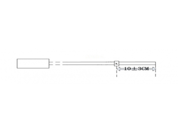
Fiber Length
Label Definition
On the module
P/N: xxxxxxxxxxx
S/N: xxxxxxxx
X=com,CH1,CH2,CH3……CHN
OthersESD Packing
RoHS and GR-1073 compliance
Related products


Send Message
Other Products


Most Recent


More

")


Other Products
 Optical Switch")

 Optical Switch")


Videos


